- 您现在的位置:买卖IC网 > Sheet目录2007 > LTC6909HMS#TRPBF (Linear Technology)IC OSC SILICON 6.67MHZ 16-MSOP
LTC6909
15
6909fa
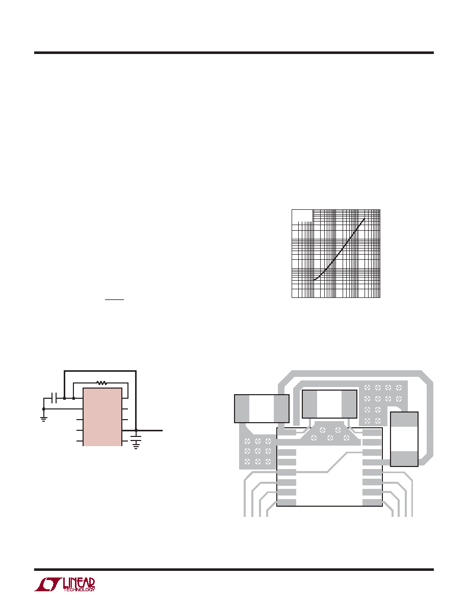
Figure 7. Start-Up Time
Figure 6. Supply Bypassing and PCB Layout
9. The connections for PH0, PH1 and PH2 are not shown
in Figure 6. These pins are connected to either GND or
V+D depending on the output phasing required for the
application. Connection to ground is done underneath
thepart.ConnectingPH2toV+Disalsostraightforward.
Connecting PH0 or PH1 to V+D may require one or
both traces to go down a layer. If you are dynamically
changing one or all of the PH pins, place a 10k resis-
tor in series with the signal line. Locate the resistor
fairly close to the PH pin. This signal typically comes
from a microcontroller or the power good signal from
a switching regulator and is usually quite noisy. The
series resistor provides some isolation between the
noisy signal and the LTC6909.
START-UP ISSUES AND CONSIDERATIONS
The start-up time and settling time to within 1% of the
final value is estimated by the following equation:
tSTART ≈RSET
25s
1k
+10s
For instance, with RSET = 100k, the LTC6909 will settle to
within 1% of its 1MHz final value in approximately 260s.
Figure7showsthestart-uptimeforvariousRSETresistors.
To assist in an orderly start-up sequence, the LTC6909’s
outputs are in a high impedance state for the first 128
master clock cycles after power-up. This ensures that
the first clock cycle is very close to the desired operating
frequency.
Powering up and down complex multiphase switching
regulator circuits is always chaotic and can have serious
system consequences if it is not done carefully. In addition
totheLTC6909’smutingoftheoutputstoensurefirstcycle
accuracy, the PH0-PH1-PH2 codes 000 (all outputs are
ApplicAtions inForMAtion
6909 F06
C1
0.1F
C2
0.1F
DIRECT, LOW IMPEDANCE
CONNECTION TO THE V+
SUPPLY
V+A
LTC6909
GND
GROUND
PLANE
GROUND
PLANE
PH0
PH1
OUT1
SET
PH2
MOD
V+D
OUT8
RSET
V+A
GND
C1
RSET
C2
PH0
PH1
OUT1
OUT2
OUT3
OUT4
SET
PH2
MOD
V+D
OUT8
OUT7
OUT6
OUT5
RSET (Ω)
100
ST
AR
T-UP
DELA
Y(s)
1000
1k
100k
1M
10M
6909 F07
10
10k
10000
TA = 25°C
V+ = 3V
发布紧急采购,3分钟左右您将得到回复。
相关PDF资料
LTC6990MPS6#TRPBF
IC VCO CONFIG GAIN/VOLT TSOT23-6
LTC6991MPS6#TRPBF
IC OSCILLATOR RESET LF TSOT23-6
LTC6992MPS6-4#TRPBF
IC OSC PWM VOLT CTLR TSOT23-6
LTC6994CDCB-2#TRPBF
IC DELAY LINE 6-DFN
LTC7541ABN#PBF
IC CMOS D/A CONV 12BIT 18-DIP
LTC7545ACG#TRPBF
IC D/ACONV MULTIPLY 12BIT 20SSOP
LTC8043EN8
IC D/A CONV 12BIT SERIAL 8-DIP
LTC8143ESW#TRPBF
IC D/A CONV 12BIT SERIAL 16-SOIC
相关代理商/技术参数
LTC6909HMS-PBF
制造商:LINER 制造商全称:Linear Technology 功能描述:1 to 8 Output, Multiphase Silicon Oscillator with Spread Spectrum Modulation
LTC6909HMS-TRPBF
制造商:LINER 制造商全称:Linear Technology 功能描述:1 to 8 Output, Multiphase Silicon Oscillator with Spread Spectrum Modulation
LTC6909IMS#PBF
功能描述:IC OSC SILICON 6.67MHZ 16-MSOP RoHS:是 类别:集成电路 (IC) >> 时钟/计时 - 可编程计时器和振荡器 系列:- 标准包装:3,000 系列:- 类型:振荡器 - 晶体 计数:- 频率:- 电源电压:2.3 V ~ 5.5 V 电流 - 电源:1.07mA 工作温度:-30°C ~ 80°C 封装/外壳:SOT-665 包装:带卷 (TR) 供应商设备封装:SS迷你型-5D 安装类型:表面贴装 其它名称:AN8955SSMTXLTR
LTC6909IMS#TRPBF
功能描述:IC OSC SILICON 6.67MHZ 16-MSOP RoHS:是 类别:集成电路 (IC) >> 时钟/计时 - 可编程计时器和振荡器 系列:- 产品培训模块:Lead (SnPb) Finish for COTS
Obsolescence Mitigation Program 标准包装:45 系列:- 类型:温度 - 补偿晶体振荡器(TCXO) 计数:- 频率:25MHz 电源电压:3.135 V ~ 3.465 V 电流 - 电源:1.5mA 工作温度:-40°C ~ 85°C 封装/外壳:16-SOIC(0.295",7.50mm 宽) 包装:管件 供应商设备封装:16-SOIC W 安装类型:表面贴装
LTC6909IMS-PBF
制造商:LINER 制造商全称:Linear Technology 功能描述:1 to 8 Output, Multiphase Silicon Oscillator with Spread Spectrum Modulation
LTC6909IMS-TRPBF
制造商:LINER 制造商全称:Linear Technology 功能描述:1 to 8 Output, Multiphase Silicon Oscillator with Spread Spectrum Modulation
LTC690C
制造商:LINER 制造商全称:Linear Technology 功能描述:Microprocessor Supervisory Circuits
LTC690CN8
功能描述:IC MPU SUPERVISORY CIRCUIT 8-DIP RoHS:否 类别:集成电路 (IC) >> PMIC - 监控器 系列:- 标准包装:1 系列:- 类型:简单复位/加电复位 监视电压数目:1 输出:开路漏极或开路集电极 复位:高有效 复位超时:- 电压 - 阀值:1.8V 工作温度:-40°C ~ 125°C 安装类型:表面贴装 封装/外壳:6-TSOP(0.059",1.50mm 宽)5 引线 供应商设备封装:5-TSOP 包装:剪切带 (CT) 其它名称:NCP301HSN18T1GOSCT